
The CMOS IC Design Process
The CMOS circuit design process consists of defining circuit
inputs and outputs, hand calculations, circuit simulations, circuit layout,
simulations including parasitics, reevaluation of circuit inputs and outputs,
fabrication, and testing. A flowchart of this process is shown in Fig. 1.1. The
circuit specifications are rarely set in concrete; that is, they can change as
the project matures. This can be the result of trade-offs made between cost and
performance, changes in the marketability of the chip, or simply changes in the
customer's needs. In almost all cases, major changes after the chip has gone
into production are not possible. This text concentrates on custom IC design.
Other (noncustom) methods of designing chips, including
field-programmable-gate-arrays (FPGAs) and standard cell libraries, are used
when low volume and quick design turnaround are important. Most chips that are
mass-produced, including microprocessors and memory, are examples of chips that
are custom designed. The task of laying out the IC is often given to a layout
designer. However, it is extremely important that the engineer can layout a
chip (and can provide direction to the layout designer on how to layout a chip)
and understand the parasitics involved in the layout. Parasitics are the stray
capacitances, inductances, pn junctions, and bipolar transistors, with the
associated problems (breakdown, stored charge, latch-up, etc.). A fundamental
understanding of these problems is important in precision/high-speed design.
 |
| Fig. 1.1 |
Fabrication:
CMOS integrated circuits are fabricated on thin circular
slices of silicon called wafers. Each wafer contains several (perhaps hundreds
or even thousands) of individual chips or "die" (Fig. 1.2.1). For
production purposes, each die on a wafer is usually identical, as seen in the
photograph in Fig. 1.2. Added to the wafer are test structures and process
monitor plugs (sections of the wafer used to monitor process parameters). The
most common wafer size (diameter) in production at the time of this writing is
300 mm (12 inches).
Note, in Fig. 1.3, that the chip's electrical signals are
transmitted to the pins of the package through wires. These wires (called
"bond wires") electrically bond the chip to the package so that a pin
of the chip is electrically connected (shorted) to a piece of metal on the chip
(called a bonding pad). The chip is held in the cavity of the package with an
epoxy resin ("glue"). The ceramic package used
isn't used for most mass-produced chips. Most chips that are mass-produced use plastic packages. Exceptions to this statement are chips that
dissipate a lot of heat or chips that are placed directly on a printed circuit
board (where they are simply "packaged" using a glob of resin).
Plastic packaged (encapsulated) chips place the die on a lead frame and then encapsulate the die and lead frame in plastic. The plastic is melted
around the chip. After the chip is encapsulated, its leads are bent to the
correct position. This is followed by printing information on the chip (the
manufacturer, the chip type, and the lot number) and finally placing the chip
in a tube or reel for shipping to a company that makes products that use the
chips. Example products might include chips that are used in cell phones,
computers, microwave ovens, printers.
 |
| Fig. 1.2 |
 |
| Fig. 1.2.1 |
 |
| Fig. 1.2.2 |
 |
| Fig. 1.3 |
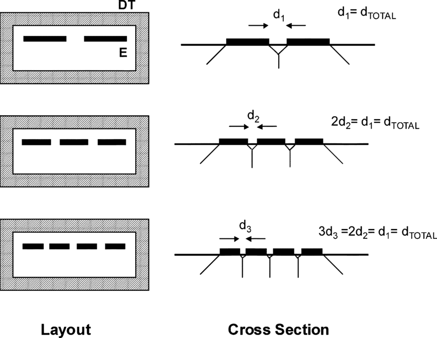
Layout
and Cross-Sectional Views:
The view that we see when laying out a chip is the top, or
layout, view of the die. However, to understand the parasitics and how the
circuits are connected together, it's important to understand the chip's
cross-sectional view. Since we will often show a layout view followed by a
cross-sectional view, let's make sure we understand the difference and how to
draw a cross-section from a layout.
The final conclusion is that layout see us that how many things
we are added and
cross-sectional view give us information regarding how
much in-depth, we added one material.
 |
| Fig. 1.4 |
References:
1) http://www.electronicsandyou.com/blog/top-silicon-wafer-manufacturing-companies-in-the-world.html
Comments
Post a Comment