
                          Sampling theorem and proof 

Statement: A continuous time signal can be represented in its samples and can be recovered back when sampling frequency fs is greater than or equal to the twice the highest frequency component of message signal. i. e.
fs2fm.

Proof: Consider a continuous time signal x(t). The spectrum of x(t) is a band limited to fm Hz i.e. the spectrum of x(t) is zero for |ω|>ωm.
Sampling of input signal x(t) can be obtained by multiplying x(t) with an impulse train δ(t) of period Ts. The output of multiplier is a discrete signal called sampled signal which is represented with y(t) in the following diagrams:
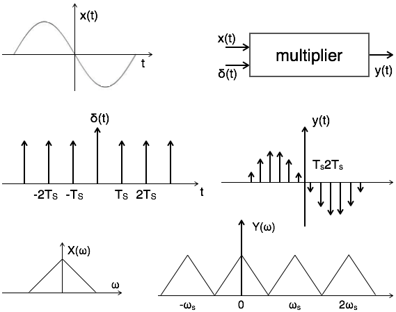
Signal Sampling
Here, you can observe that the sampled signal takes the period of impulse. The process of sampling can be explained by the following mathematical expression:
The trigonometric Fourier series representation of Î´(t) is given by
Where 
Substitute above values in equation 2.
Substitute δ(t) in equation 1.
y(t)=x(t).δ(t)
Take Fourier transform on both sides.
To reconstruct x(t), you must recover input signal spectrum X(ω) from sampled signal spectrum Y(ω), which is possible when there is no overlapping between the cycles of Y(ω).
Possibility of sampled frequency spectrum with different conditions is given by the following diagrams:

Sampling

Aliasing Effect

    Aliasing a phenomena in which high frequency components are interference with each other  to due to inadequate sampling frequency

                                   Ex- fs <2fm  

The overlapped region in case of under sampling represents aliasing effect, which can be removed by
  • considering fs >2fm
  • By using anti aliasing filters.

Comments

Popular posts from this blog

Tutorial on EasyEDA desktop software for PCB and schematic design

In this article, I am going to write a tutorial on how to use EasyEDA desktop application for creating a schematic and for PCB design. One of best advantage of this software is that you can create design offline and can automatically synchronize your design with your online EasyEDA account.  It can be used for circuits simulation, PCB deign and electronics circuits design. You can download EasyEDA desktop application by clicking on following link and it will work on windows 7 or its greater version. They are also releasing soon offline application OSX and Linux users. So keep visiting their website for more information.                                                    https://easyeda.com/page/download So let’s start and see how to design a schematic and PCB using EasyEDA offline desktop application. So first of all lets see how to create a schema...

What is Solar System Components & Installation Guide

Hello Dear Reader, Here in this post, I will give an idea about installation cost analysis of Solar PV System. I hope you read this post regarding the calculation of solar PV system  so in this post I have given an approximate cost analysis of the different solar system installations.  What is Solar System Components Solar systems are made up of solar panels (modules), a mounting system, and a solar inverter with computerised controller. Solar panels produce DC electricity from sunlight. Then the inverter converts the generated electricity into AC, so that it can be used in the household. The computerised controller manages the solar system and ensures optimal performance. If you want a battery backup system or an off-the-grid solar system, a battery is required. What is a Solar Energy System? Solar Energy System consists of 4 main components that decide the working of a solar energy system. Solar Panel Solar Inverter Solar Battery Panel Stand, and Solar Panel Installation...

CMOS OPAMP Design Using LTspice

  Hello Dear Reader, Here in this post, I will give an idea about how CMOS OPAMP designing using 180nm technology node and using LTspice. from that opamp I have design switched capacitor integrator. Design Specifications: Here Design specification may be changed according to the application here my target is to design an active lowpass filter so I have chosen an opamp integrator so in the below I have explained how to design an opamp as well as an integrator in a 180nm technology node in LTspice. So let's start design First, we need a technology parameter file so that the file we can insert in the LTspice, in my example it is 180nm so mostly it is available from the  http://ptm.asu.edu/latest.html  and you make one text file using notepad or whatever is fit on your own. Then go to the LTspice and new schematic and then you see .op on the right most upper side click on it and give your text file path after .include  as shown in the below images.  Now first of all...